
Revolutionizing Wafer Packaging: A Deep Dive into Advanced Technologies
The Future of Wafer Packaging: Innovative Solutions for Semiconductor Industry
In the rapidly evolving semiconductor industry, the importance of efficient and reliable wafer packaging cannot be overstated. As chips become smaller, more powerful, and increasingly complex, the need for advanced packaging solutions has become paramount. In this article, we will explore the latest trends in wafer packaging technology and how they are revolutionizing the way semiconductor devices are manufactured and assembled.
The Rise of Fan-Out Wafer Level Packaging
One of the most significant advancements in wafer packaging technology is the adoption of fan-out wafer level packaging (FOWLP). This cutting-edge packaging method allows for the integration of multiple chips on a single wafer, offering improved performance and efficiency compared to traditional packaging techniques. With FOWLP, semiconductor manufacturers can achieve higher levels of miniaturization and form factor flexibility, paving the way for the development of smaller and more powerful devices.
3D Integration: Redefining Wafer Packaging
Another groundbreaking innovation in wafer packaging is 3D integration, which involves stacking multiple semiconductor layers on top of each other to create vertically integrated circuits. By utilizing 3D integration techniques, manufacturers can significantly increase chip density and performance while reducing power consumption and latency. This approach not only enhances the overall functionality of semiconductor devices but also enables the development of complex and feature-rich applications.
Wafer-on-Wafer Technology: Unleashing the Full Potential of Semiconductor Devices
Wafer-on-wafer (WoW) technology is poised to revolutionize wafer packaging by enabling the direct integration of multiple wafers into a single device. This innovative approach allows for the seamless interconnection of different semiconductor materials and processes, resulting in enhanced device performance and functionality. By eliminating the need for complex interposers and connectors, WoW technology simplifies the manufacturing process and reduces overall production costs, making it an attractive option for semiconductor manufacturers.
Conclusion
In conclusion, the future of wafer packaging is filled with promise and potential, thanks to innovative technologies such as fan-out wafer level packaging, 3D integration, and wafer-on-wafer technology. As the demand for faster, smaller, and more efficient semiconductor devices continues to grow, the development of advanced packaging solutions will play a crucial role in shaping the future of the industry. By embracing these cutting-edge technologies, semiconductor manufacturers can unlock new possibilities and drive the next wave of innovation in wafer packaging.


-
 01
01Further Discussion About Protein Bar Packing Machinery
27-02-2024 -
 02
02Sustain The Best Crispy With Automatic Packaging Machines
29-01-2024 -
 03
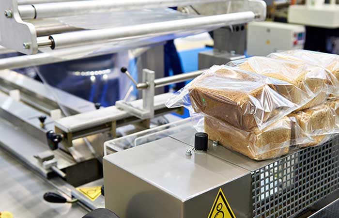
03Bread Packing Machine For Bakery Business
19-01-2024 -
 04
04How Flow Wrappers Are Adapting to Changing Trends
01-11-2023 -
 05
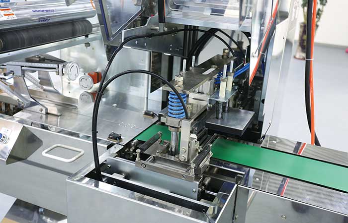
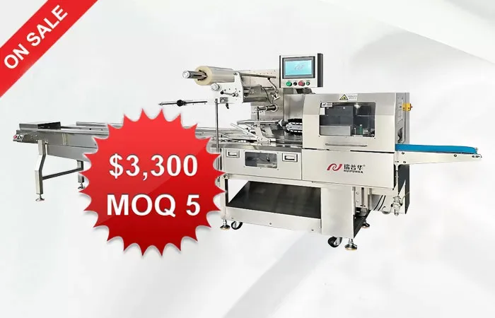
05The Comprehensive Guide to Packaging Machinery
31-10-2023 -
 06
06Automatic Cookie Packaging System Performance
01-09-2023 -
 07
07Streamlining Biscuit Packaging with Multipack Biscuit Packaging Machines
25-08-2023 -
 08
08From Assembly To Shipping: The Energy Bar Packaging Machine Does All
28-02-2023 -
 09
09Maximizing Efficiency With Food Packaging Machine Technology
22-02-2023 -
 10
10Clients Hunt For Professional And Functional Packaging Machine
10-11-2022
