
Revolutionizing Semiconductor Packaging: The Future of Wafer Packaging Systems
The Future of Wafer Packaging Systems
In the ever-evolving landscape of semiconductor technology, wafer packaging systems play a pivotal role. As the demand for smaller, faster, and more energy-efficient devices continues to rise, the need for innovative wafer packaging solutions becomes increasingly apparent. Let’s delve into the world of wafer packaging and explore the trends shaping its future.
Miniaturization and Integration
One of the key trends driving the evolution of wafer packaging systems is miniaturization. As consumers demand sleeker and more compact electronic devices, manufacturers are under pressure to pack more functionality into smaller spaces. This has led to the development of advanced packaging techniques such as wafer-level chip-scale packaging (WLCSP) and fan-out wafer-level packaging (FOWLP).
Advanced Materials
Another area of innovation in wafer packaging systems is the use of advanced materials. From ultra-thin substrates to high-conductivity metals, manufacturers are constantly exploring new materials to enhance the performance and reliability of semiconductor packages. Novel materials like silicon interposers and copper pillars are enabling the next generation of high-density, high-speed, and high-bandwidth devices.
3D Integration
3D integration is revolutionizing wafer packaging by enabling the stacking of multiple chips vertically. This vertical integration offers benefits such as reduced footprint, shorter interconnect lengths, and improved performance. Through technologies like through-silicon vias (TSVs) and microbumps, 3D-integrated packages are paving the way for more efficient and powerful devices.
The Rise of Heterogeneous Integration
Heterogeneous integration is blurring the lines between different semiconductor technologies. By combining diverse components like logic, memory, and sensors on a single wafer, manufacturers can create highly integrated systems with enhanced functionality. This trend is driving the development of multi-chip modules (MCMs) and system-in-package (SiP) solutions that offer superior performance in a compact form factor.
Challenges and Opportunities
While the future of wafer packaging systems holds immense promise, it also presents challenges. From thermal management issues to signal integrity concerns, manufacturers are faced with a myriad of technical hurdles to overcome. However, these challenges also bring opportunities for innovation and collaboration across the semiconductor industry.
Conclusion
The future of wafer packaging systems is bright, fueled by a relentless pursuit of technological advancement. As manufacturers continue to push the boundaries of what is possible, we can expect to see even more groundbreaking innovations in the world of semiconductor packaging.


-
 01
01Further Discussion About Protein Bar Packing Machinery
27-02-2024 -
 02
02Sustain The Best Crispy With Automatic Packaging Machines
29-01-2024 -
 03
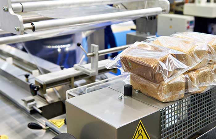
03Bread Packing Machine For Bakery Business
19-01-2024 -
 04
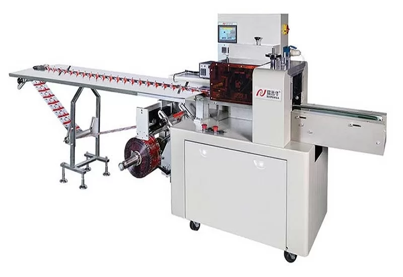
04How Flow Wrappers Are Adapting to Changing Trends
01-11-2023 -
 05
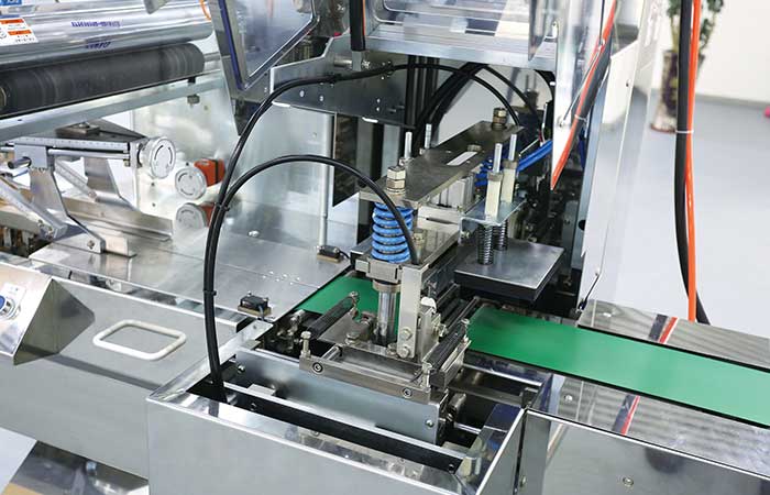
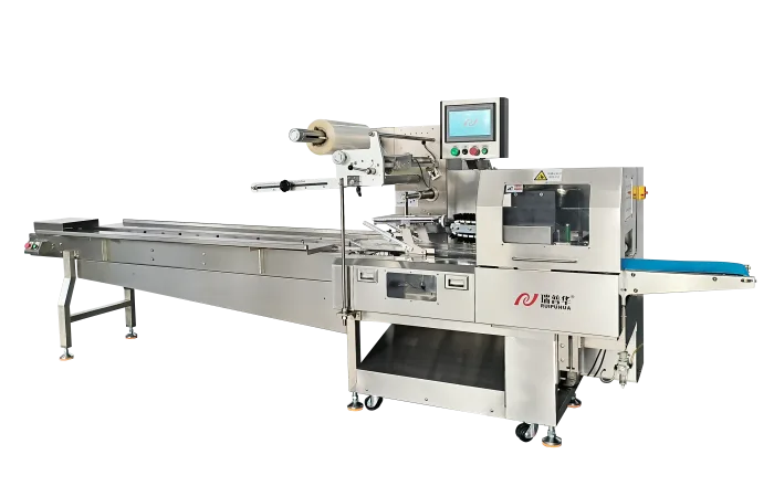
05The Comprehensive Guide to Packaging Machinery
31-10-2023 -
 06
06Automatic Cookie Packaging System Performance
01-09-2023 -
 07
07Streamlining Biscuit Packaging with Multipack Biscuit Packaging Machines
25-08-2023 -
 08
08From Assembly To Shipping: The Energy Bar Packaging Machine Does All
28-02-2023 -
 09
09Maximizing Efficiency With Food Packaging Machine Technology
22-02-2023 -
 10
10Clients Hunt For Professional And Functional Packaging Machine
10-11-2022
