
Revolutionizing Semiconductor Packaging: A Dive into Advanced Wafer Packaging Systems

The Rise of Wafer Packaging Systems
In the realm of semiconductor technology, the evolution of wafer packaging systems stands as a testament to progress in microelectronics. The integration of advanced packaging techniques has paved the way for smaller, faster, and more efficient electronic devices.
Wafer-level packaging (WLP) has emerged as a game-changer in the semiconductor industry. By encapsulating individual integrated circuits at the wafer level, WLP offers significant advantages in terms of size reduction, enhanced electrical performance, and improved thermal management.
The Role of Fan-Out Wafer-Level Packaging (FO-WLP)
One of the most prominent trends in wafer packaging systems is the adoption of Fan-Out Wafer-Level Packaging (FO-WLP). This technology enables the redistribution of I/O pads across a larger area, providing increased flexibility in chip design and improved signal integrity.
FO-WLP offers a cost-effective solution for achieving higher levels of integration while maintaining excellent electrical performance. By eliminating the need for traditional packaging substrates, FO-WLP reduces overall package size and enhances system reliability.
Advancements in 3D IC Integration
Another area of innovation in wafer packaging systems is the development of 3D IC integration technologies. By stacking multiple dies vertically, 3D ICs enable higher interconnect densities and shorter signal paths, resulting in improved performance and power efficiency.
Through the use of Through-Silicon Vias (TSVs) and microbumps, 3D IC technology enables seamless connectivity between stacked dies, creating a more compact and energy-efficient solution for complex electronic systems.
Exploring the Future of Wafer Packaging Systems
As we look to the future, the continued advancement of wafer packaging systems holds great promise for the semiconductor industry. From the development of novel materials to the integration of new manufacturing processes, innovation in wafer packaging is driving the next generation of electronic devices.
Exciting prospects such as wafer-scale integration, heterogeneous integration, and advanced interconnection technologies are set to redefine the boundaries of what is possible in semiconductor packaging. With each new breakthrough, we move closer to a world where electronics are smaller, faster, and more interconnected than ever before.


-
 01
01Further Discussion About Protein Bar Packing Machinery
27-02-2024 -
 02
02Sustain The Best Crispy With Automatic Packaging Machines
29-01-2024 -
 03
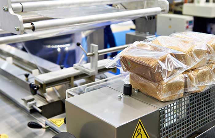
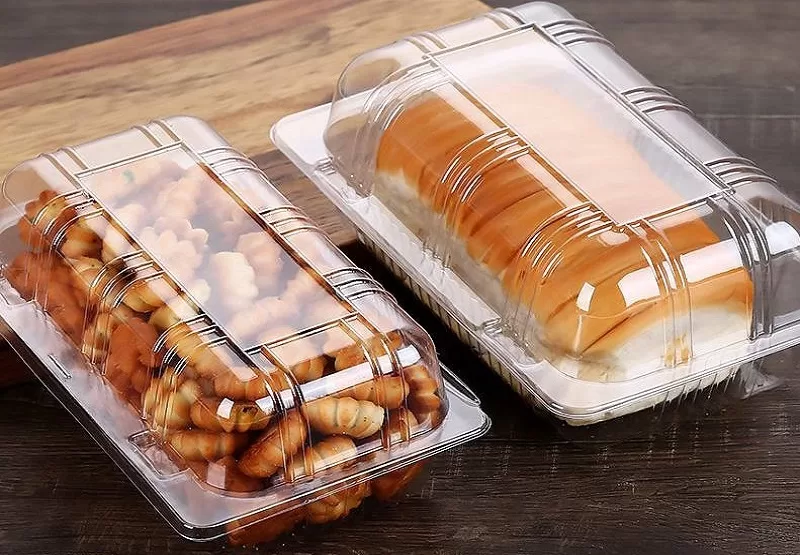
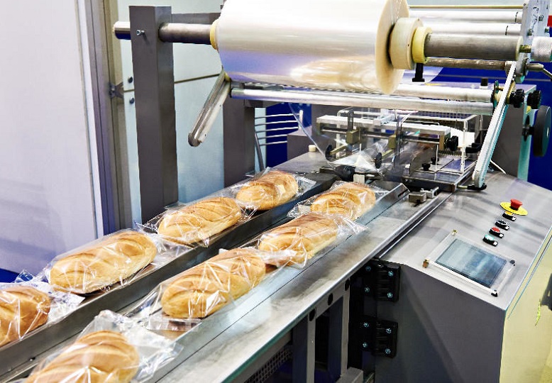
03Bread Packing Machine For Bakery Business
19-01-2024 -
 04
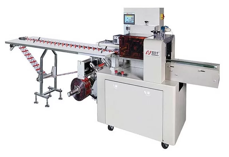
04How Flow Wrappers Are Adapting to Changing Trends
01-11-2023 -
 05
05The Comprehensive Guide to Packaging Machinery
31-10-2023 -
 06
06Automatic Cookie Packaging System Performance
01-09-2023 -
 07
07Streamlining Biscuit Packaging with Multipack Biscuit Packaging Machines
25-08-2023 -
 08
08From Assembly To Shipping: The Energy Bar Packaging Machine Does All
28-02-2023 -
 09
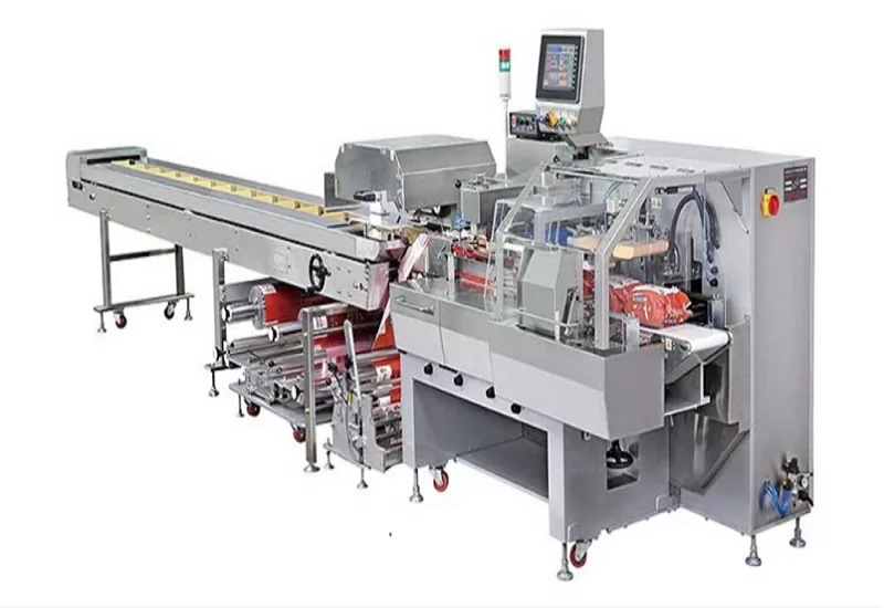
09Maximizing Efficiency With Food Packaging Machine Technology
22-02-2023 -
 10
10Clients Hunt For Professional And Functional Packaging Machine
10-11-2022
