
Revolutionizing Wafer Packaging: A Future-Ready Approach
Revolutionizing Wafer Packaging: A Future-Ready Approach
In the world of semiconductor manufacturing, the importance of wafer packaging cannot be understated. As technology advances, the demand for smaller, faster, and more efficient chips continues to grow. This has led to a significant evolution in wafer packaging techniques, with an emphasis on innovative solutions that can meet the demands of today’s electronics industry.
One of the key challenges in wafer packaging has been the need for greater density and miniaturization. Traditional packaging methods have often struggled to keep up with the demand for smaller and more powerful devices. However, with advancements in technology, new packaging solutions are emerging that offer a range of benefits, from improved performance and reliability to enhanced durability and cost-effectiveness.
One such innovation is the development of 3D wafer stacking technologies, which allow multiple layers of chips to be stacked on top of each other, creating a compact and efficient packaging solution. This approach not only reduces the overall footprint of the final product but also improves thermal management and signal integrity, leading to better overall performance.
Another trend in wafer packaging is the move towards fan-out wafer-level packaging. This technique involves redistributing the connection points on the wafer, allowing for more compact and efficient designs. By eliminating the need for wire bonding, fan-out wafer-level packaging offers improved electrical performance and higher interconnect densities, making it an attractive option for high-performance applications.
Furthermore, the integration of advanced materials such as organic substrates and flexible substrates is revolutionizing wafer packaging. These materials offer improved electrical characteristics, thermal management, and signal integrity, making them ideal for applications where performance and reliability are paramount. Additionally, the use of advanced manufacturing techniques such as laser ablation and additive manufacturing is enabling the development of more complex and customized packaging solutions.
As the demand for smaller, faster, and more powerful electronic devices continues to rise, the need for innovative wafer packaging solutions will only grow. By embracing new technologies and materials, manufacturers can develop packaging systems that not only meet current requirements but also pave the way for future advancements in semiconductor manufacturing.


-
 01
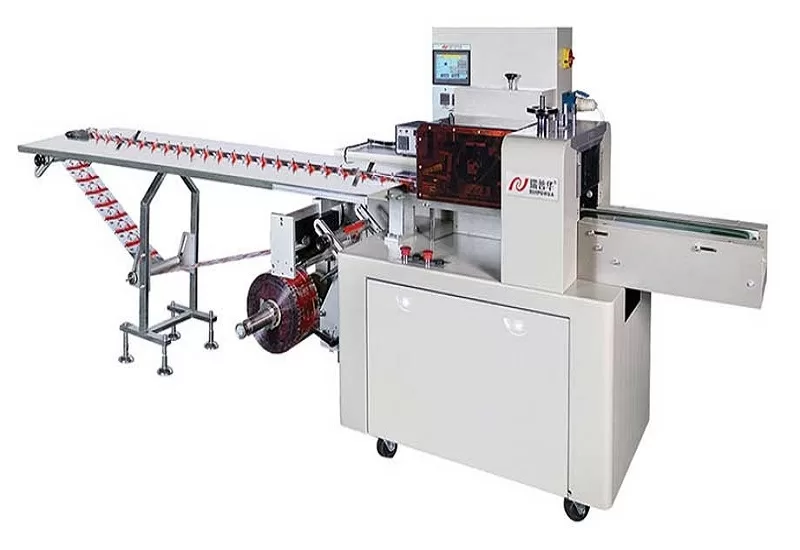
01Further Discussion About Protein Bar Packing Machinery
27-02-2024 -
 02
02Sustain The Best Crispy With Automatic Packaging Machines
29-01-2024 -
 03
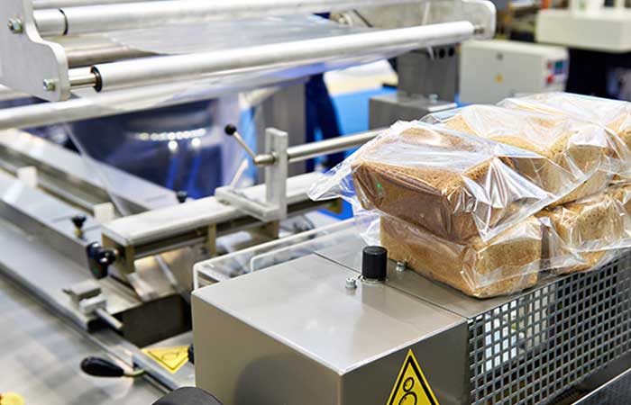
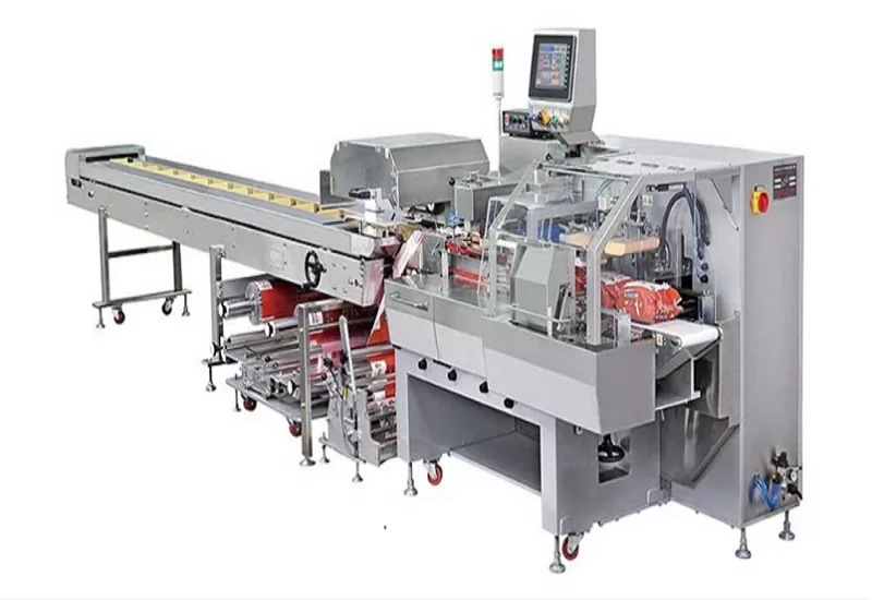
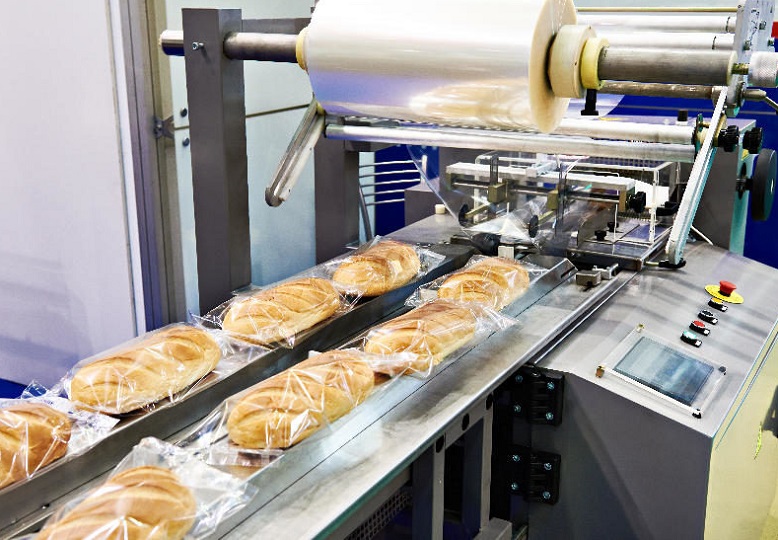
03Bread Packing Machine For Bakery Business
19-01-2024 -
 04
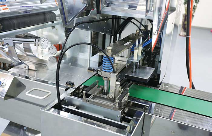
04How Flow Wrappers Are Adapting to Changing Trends
01-11-2023 -
 05
05The Comprehensive Guide to Packaging Machinery
31-10-2023 -
 06
06Automatic Cookie Packaging System Performance
01-09-2023 -
 07
07Streamlining Biscuit Packaging with Multipack Biscuit Packaging Machines
25-08-2023 -
 08
08From Assembly To Shipping: The Energy Bar Packaging Machine Does All
28-02-2023 -
 09
09Maximizing Efficiency With Food Packaging Machine Technology
22-02-2023 -
 10
10Clients Hunt For Professional And Functional Packaging Machine
10-11-2022
